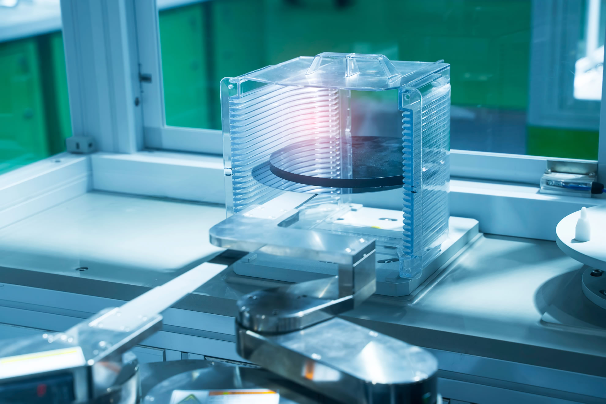
THIN FILM DIELECTRIC PECVD
PECVD (Plasma Enhanced Chemically Evaporated Deposition) are useful Low Temperature dielectrics that offer many applications ability to isolate metal layers, while maintaining low temperature over a specific metal. PECVD offers flexible single sided depositions over a wide range of materials. Used in Semiconductor, Bio-Medical, MEMS and many more applications.
Low Temperature PECVD SiO2 (Silane Based) (R.I. 1.5 +/-0.3) 380 Degree C
400A-5KA +/-5%
5KA-10KA +/-5%
10KA-20KA +/-5%
PECVD Oxy-Nitride (R.I. 1.7 +/-0.2)
400A-3KA +/-5%
3KA-5KA +/-5%
Round Substrates:
| 50mm | 2 inch |
| 100mm | 4 inch |
| 125mm | 5 inch |
| 150mm | 6 inch |
| 200mm | 8 inch |
Square Substrates:
156mm X 156mm & Smaller
Coupons can be run on a carrier wafer
Note:
Noel utilizes a Variable, Dual Frequency Tool: 1250W @>1300 MHZ/750W @100-400 kHz.
All film deposition as measured on a silicon test wafer.
Multi-sack depositions are measured on the individual film, utilizing a test wafer,
A uniformity map will be provided for each film.
Noel is responsible for the film deposition, uniformity and thickness.
Noel is not responsible for results of multi-stack depositions.
R.I. as measured on bare test wafers for 1KA thickness.